What if students could design real chips, run them on silicon and learn hands-on with no expensive tools? India’s new open source PDK flow is making it possible.
Access to advanced chip design tools has been a barrier for many students and researchers in India, especially those in tier II, III, and IV colleges, who have Indian process design kits (PDKs) but lack high-end proprietary electronic design automation (EDA) tools. To bridge this gap and enable hands-on learning, VSD (VLSI System Design) has successfully mapped an Indian PDK to an open source flow, allowing students to complete full RTL-to-GDS chip design cycles and test on real silicon.

Kunal Ghosh, founder of VSD, hosted a webinar on 8 February 2026 to announce the milestone. The initiative lets students use Indian PDKs with open source EDA tools to gain hands-on experience and create silicon-proven designs without costly proprietary software.
“This opens up an entire learning path for students aspiring to design and tape out chips within India,” Ghosh said during the webinar. He emphasised the importance of ‘silicon-proven flows,’ highlighting how hands-on experience with real chips significantly improves industry readiness.
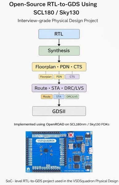
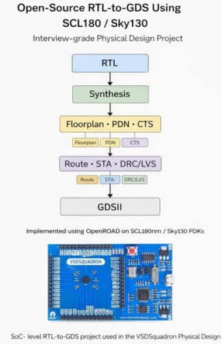
During the webinar, a project demonstration was shown. The conversion of the SkyWater 130 nm Caravel chip design to the SCL 180 nm PDK was entirely completed using open source tools. The converted design, known as VSD Caravel, preserves full functionality and is bounded by general-purpose I/Os, making it suitable for educational and experimental purposes.
“This effort took over five years and involved close collaboration between students, experts, the PDK team, and the open source community,” Kunal added. “It is a proud moment for the Indian semiconductor community and a step forward in building local design capabilities.”
He also detailed how critical elements such as metal sizing, orientation, clock-gating cells, full adders, and parasitic extraction were handled. He stressed that identifying correct cell functions and mapping them across technology nodes is key to maintaining performance and power efficiency. Currently, parasitic extraction relies on estimated resistance-capacitance (RC) values, but full accuracy is expected once proprietary resistance-capacitance extraction (RCX) patterns are incorporated.
“Students, from undergraduates to advanced researchers, can now get hands-on experience with real-world chip design processes,” said Kunal. The program also includes optional post-six-week tasks on hierarchical placement and routing, providing participants with insight into full-chip integration.
All flow scripts, pre-compiled binaries, and configuration files are available through a GitHub repository, with virtual network computing (VNC)-enabled graphical user interface (GUI) access for real-time layout inspection. While analogue design and antenna rule enforcement are still under development, the team plans to extend support in the coming months.
The initiative positions India’s engineering community at the forefront of open source chip design, enabling participants to explore complex technology nodes without relying solely on commercial EDA tools, a significant step toward building local expertise in semiconductor design.