A single platform brings multiple DC-DC regulators together, helping you test performance, compare topologies, validate behavior, and move from evaluation to design integration.
The Building Block Solutions – Switchers (BBS-SW) reference design from Microchip is designed to help engineers quickly evaluate and compare different DC-DC switching regulators in one place. It brings together multiple converter types on a single platform, making it easier to test real performance, check compatibility, and move toward integration without building separate test setups for each device.
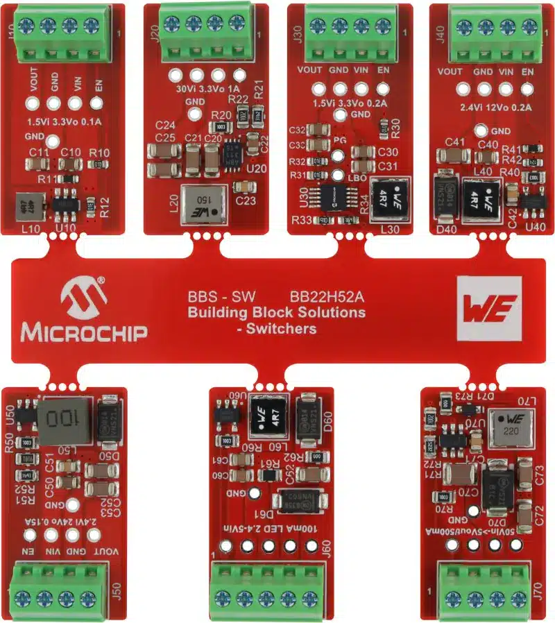
At its core, the board contains seven independent sub-modules, each based on a different monolithic DC-DC regulator. This structure allows side-by-side testing of different topologies such as boost and buck converters. Engineers can power each section independently, probe signals, and observe how each regulator behaves under different loads and input conditions.

The platform includes multiple boost regulator configurations. One of them is designed for low quiescent current operation and supports both PFM and PWM modes, along with output disconnect and bypass options. This makes it useful for systems that run on batteries and need efficient voltage boosting at low power levels. Another boost section provides a fixed 3.3V output and includes features such as programmable low battery detection, under-voltage lockout, and automatic bypass from input to output. This setup is suitable for powering microcontrollers and sensor nodes directly from low-voltage sources.
For applications that require higher voltage rails, the board includes two boost converters built around high-voltage integrated switches. These are configured to generate 12V and 24V outputs. Both include PWM control and under-voltage lockout, allowing engineers to study how higher voltage conversion behaves from low input supplies and how stability is maintained across conditions.
On the step-down side, the board integrates buck regulators for common use cases. One section supports input voltages up to 30V and delivers up to 1A output, which fits embedded systems that need efficient voltage reduction. Another buck converter provides a regulated 5V output, which aligns with logic circuits and USB-powered designs.
The board also includes a step-up LED driver that can supply up to 100 mA. It supports features like under-voltage lockout and open-load protection, allowing safe operation while driving multiple LEDs with a combined forward voltage below 25V. This helps in evaluating lighting and indication circuits without needing a separate driver design.
The modular layout simplifies the evaluation process. Each sub-module is clearly separated and labeled, so engineers can focus on one converter at a time. Pre-configured output voltages reduce setup effort, while built-in test points and connectors make it easy to take measurements, inject signals, and connect the board into a larger system.
Using this reference design, design engineers can compare efficiency across different converters, validate startup and transient response, and test behavior under varying loads. It also helps in selecting the right topology for a given application, verifying component choices, and reducing risk before committing to a custom PCB. Engineers can reuse proven sections of the design, adapt layouts, and shorten development cycles. The board also serves as a practical tool to understand switching regulator behavior through direct measurement rather than simulation alone.
Microchip has tested this reference design. It comes with a bill of materials (BOM), schematics, assembly drawing, printed circuit board (PCB) layout, and more. The company’s website has additional data about the reference design. To read more about this reference design, click here.