A new development in chip packaging could change how AI processors are built, making them smaller, faster, and more stable in data centers.

Kyocera Corporation has commercialized a new multilayer ceramic core substrate for advanced semiconductor packages, targeting high-performance processors such as xPUs and switch ASICs as AI data centers demand larger, denser, and more powerful chip architectures.

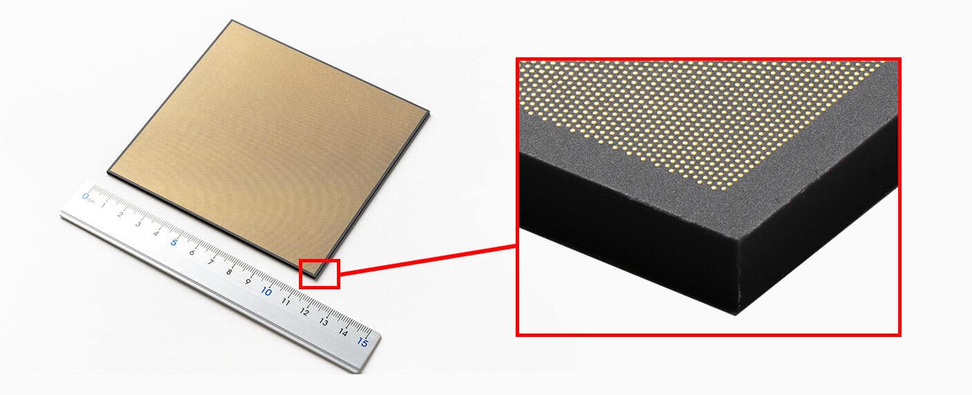
Built on Kyocera’s proprietary Fine Ceramic materials, the substrate is designed to address one of the semiconductor industry’s growing packaging challenges: warpage. As chip packages expand to support higher integration and faster processing—particularly in advanced 2.5D architectures—even minor substrate deformation can affect assembly precision, reliability, and performance.
The ceramic core substrate combines higher structural rigidity with high-density multilayer wiring, giving chipmakers an alternative to conventional organic core substrates, which become more prone to bending and design limitations as package sizes increase. Kyocera says the added rigidity reduces warpage during mounting and can support thinner substrate designs, potentially improving both device performance and package miniaturization.
The new substrate also enables finer wiring through its ceramic manufacturing process. Unlike organic substrates, where vias are drilled after the material is formed, ceramic vias are created while the material is still pliable before sintering. That allows for smaller via diameters and tighter spacing, making it easier to build dense three-dimensional interconnects needed for next-generation AI and high-speed networking chips.
The launch comes as generative AI and large language models drive rapid expansion in global AI infrastructure, increasing demand for high-performance xPUs and ASICs. Those chips increasingly rely on advanced packaging techniques such as 2.5D integration, where multiple chips are mounted side-by-side on a high-density interposer to improve bandwidth and processing efficiency.
To support adoption, Kyocera is also offering custom design and simulation services, including thermal, electrical, and warpage analysis, to help customers optimize package performance earlier in the development cycle.
The product expands Kyocera’s semiconductor packaging portfolio as manufacturers look for new substrate technologies to keep pace with rising performance requirements and increasing package complexity.
Click here for the original announcement.