
What kinds of jobs are emerging from the massive investments in India’s semiconductor industry? Do we have the talent to meet this demand? If not, how are the government, academia, and industry addressing the gap—and how can these efforts be accelerated to build the right talent faster? To explore these questions, EFY’s Rahul Chopra had the opportunity to speak with Dr Ashwini K Aggarwal, a seasoned leader who has worn many hats within the semiconductor ecosystem. Here is what he shared.

Q. What kind of job opportunities or career opportunities are emerging now because of the growth in the semiconductor sector and all the investments happening?
A. The semiconductor industry in India is reaching an inflection point. With major mega and giga projects announced, we are seeing investments of close to ₹150 billion being implemented. Tata’s fab is progressing at a great pace. Projects from companies such as Kaynes, Micron, CG Semi, and many smaller players are also taking shape.
As this unfolds, it is inevitable that India will need to develop manufacturing skills. While India has long been designing chips, we now need to design our future in the ‘Make in India’ era. Careers are evolving, and we are seeing growing demand for skilled professionals across the entire ecosystem, not just at fabs but throughout the value chain.
Q. Can you give some examples of the kinds of jobs being created?
A. Let me quote the CEO of Applied Materials. In a meeting, he once said, “I wish I had people who knew atomic layer deposition or could understand plasma engineering in the country; I would give 10 job letters on the spot.”
Design remains key, no doubt. But we are now completing the circle with manufacturing. A fab, as a process industry, requires more than electronics engineers—it also needs mechanical, materials, chemical, computer, electrical, and EHS (environment, health, and safety) engineers.
Each of these disciplines plays a crucial role in enabling the successful operation of a fab. In addition to technical roles, there is a significant demand for professionals in health and safety. Specialists who manage hazardous chemicals and factory operations are critical. These skills are also highly transferable. An industrial safety engineer trained in semiconductor manufacturing can work in the chemical sector or take on roles abroad.
Q. What other types of units are emerging to support the semiconductor ecosystem in India?
A. Applied Materials and Lam Research have both announced major investments. Applied Materials began with a $400 million project in India. They have already acquired a ₹3.5 billion land parcel in Bengaluru to build a supplier and test ecosystem. This is prompting their global supply chain partners to take India seriously. For instance, Rockwell Automation has announced a $66 million project in Chennai to build intelligent power systems for Applied’s global equipment. That is just one example; similar developments are also taking place with other companies.
Fabs also need speciality gases, bulk gases, ultra-pure water, sensors, and much more. Water technology becomes especially critical, precision in every drop leads to profit in every wafer. Even cleanroom creation and maintenance are specialised engineering functions.
| Dr Ashwini K Aggarwal is currently a Professor of Practice at Manav Rachna International Institute of Research & Studies (Faridabad/Delhi NCR); Sr Member IEEE; Founder Chair IEEE EPS, Delhi-NCR Chapter. He is also the Country Advisor of Society for Information Display. He has over 42 years of industry experience – over a decade at Applied Materials—a world leader in Semiconductor Equipment. He has co-authored the AICTE curriculum for Semiconductor manufacturing electives and is the chair of the Semiconductor manufacturing skill committee at Electronics Sector Skill COuncil. He is also the chair of the manufacturing skills committee for semiconductor packaging under MEITY-ISM advisor (packaging). |
Q. Could you elaborate more on the engineering behind fabs? What exactly happens beneath the cleanroom?
A. Sure. The real engineering beauty of a fab lies in the sub-fab, which is located below the cleanroom. This is where utility feeds, gas pipelines, safety systems, and abatement systems are installed. It involves extremely detailed industrial engineering. Even before construction begins, industrial engineers must map out the piping, feeds, sensor placements, scrubbers, and more. Every element must be pre-designed to ensure safety and maximise yield. It goes far beyond using EDA tools; precision engineering is required to build the infrastructure itself.
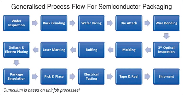
Q. How do you see India overcoming the challenge of creating new skill sets, updating curriculums, and exposing students to new equipment and tools?
Oops! This is an EFY++ article, which means it’s our Premium Content. You need to be a Registered User of our website to read its complete content.
Good News: You can register to our website for FREE! CLICK HERE to register now.
Already a registered member? If YES, then simply login to you account below. (TIP: Use ‘forgot password’ feature and reset and save your new password in your browser, if you forgot the last one!)