

What if a near-invisible layer of carbon was the very thing holding back your electric vehicle or smart grid from becoming more efficient? That’s exactly what Cornell researchers uncovered—and solved.
Imagine designing powerful new electronics—only to find that sometimes they work beautifully and sometimes not at all. That’s the dilemma scientists faced with beta gallium oxide, a promising semiconductor touted for future electric vehicles and power grids. Despite its ultra-wide band gap and high-voltage potential, devices built with it showed unpredictable performance. Why? No one had a clear answer—until now.
Cornell researchers have pinpointed the hidden saboteur: a nanometer-thin layer of carbon contamination, often left behind by fabrication methods or even just air. This microscopic barrier disrupts the critical metal-semiconductor interface, choking current flow in the very devices meant to deliver power efficiently.
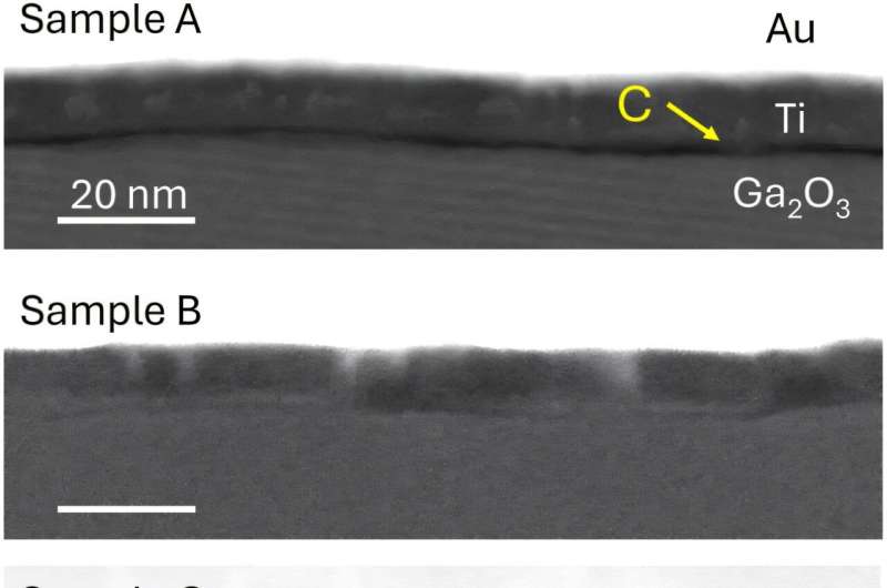
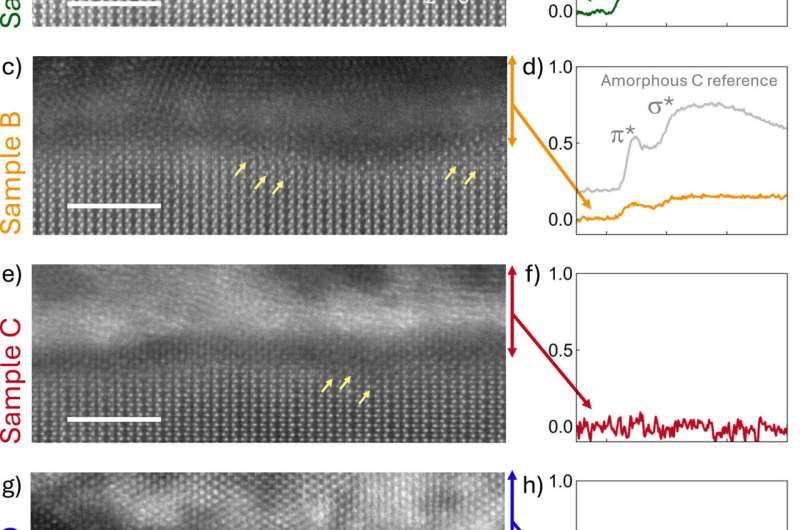
Doctoral researcher Naomi Pieczulewski and team went digging—at the atomic level. Using scanning transmission electron microscopy and advanced imaging, they compared two standard ways of applying metal contacts to beta gallium oxide: the conventional lift-off method and a metal-first approach.
What they found was eye-opening. The lift-off samples showed residual carbon trapped between the metal and semiconductor, a leftover from photoresist materials. Meanwhile, even the metal-first process wasn’t immune—air exposure introduced carbon too.
The team didn’t stop at diagnosis—they delivered a cure. A one-hour UV-ozone treatment removed the carbon from lift-off samples, achieving an ultra-low contact resistance of just 0.05 ohm-millimeters—among the lowest ever reported for non-alloyed gallium oxide. A simple five-minute active oxygen process cleaned the metal-first interfaces as well.This collaborative effort united all seven co-PIs from the AFRL-Cornell ACCESS Center, with contributions from Boise State and Micron via the Semiconductor Research Corporation.
“This is a step-change for ultra-wide bandgap electronics,” said Pieczulewski. “It’s not flashy, but it’s foundational for moving gallium oxide devices from lab to real-world applications.”