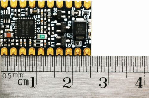
The design uses two signals to control current more accurately, changes them into a smooth voltage, and works safely with microcontrollers in small systems.

The MAXREFDES1161 reference design from Analog Devices (ADI) controls the current loop output using two separate PWM signals from a microcontroller. One signal manages coarse 8-bit adjustments, while the other handles fine 8-bit adjustments. Together, they drive precise current control.
Inside the MAX12900, the amplifier, combined with external components, forms a multi-feedback low-pass filter. This filter smooths the combined PWM signals into a steady DC voltage that sets the output current. The control loop includes a low-drift amplifier and an external transistor to maintain stable current. Another built-in amplifier measures the loop current and sends an analog signal to a microcontroller’s ADC for monitoring.
A PWM conditioner circuit inside the MAX12900 converts the digital PWM signals into a voltage that swings between the internal reference and ground, relaxing the logic level requirements. These signals pass through the low-pass filter to become a stable analog voltage.
The circuit is powered by a 24V loop supply. A resistor limits inrush current at startup, and the built-in voltage regulator steps this down to 3.3V for internal use. Two external resistors define the regulator’s output level. At startup, the amplifier and PWM outputs remain in a high-impedance state until the 3.3V supply reaches 90% of its rated value. After a short delay of 0.7 milliseconds, the power-good signal is activated.
A dual transistor, controlled by this power-good signal, acts as a switch between the 3.3V internal supply and the external output line. This same line powers the comparators and can also supply connected sensors or other devices.
This dual-PWM approach removes the need for a traditional DAC while still providing high-resolution analog output. It simplifies system design by using basic microcontroller I/O. The multi-feedback low-pass filter ensures that fast digital signals are reliably converted into clean analog voltages without additional filtering stages.
With onboard current measurement and ADC compatibility, the system allows seamless integration with microcontroller-based monitoring or feedback loops. The 2.5V reference and comparator setup improve system safety by enabling supply voltage checks and other system-level monitoring functions without extra circuitry. The startup sequence with power-good control ensures that external components receive power only after the internal system is stable. This avoids unpredictable behavior during power-up.
Designers get precise and stable current control using simple PWM signals—ideal for low-cost, compact systems. Integrated filtering and reference functions reduce the need for external components, saving board space and design time. Built-in monitoring features and intelligent power control add safety, flexibility, and reliability to industrial or embedded applications. The final result is a ready-to-use reference design that helps engineers build smarter analog output modules with minimal external circuitry and easy microcontroller interfacing.
ADI has tested this reference design. It comes with a bill of materials (BOM), schematics, assembly drawing, printed circuit board (PCB) layout, and more. The company’s website has additional data about the reference design. To read more about this reference design, click here.


