
A new solvent-based UV patterning technique enables high-resolution 2D semiconductor circuits without harsh chemicals or high temperatures, offering a sustainable path for next-generation chip fabrication.

Researchers from the Ulsan National Institute of Science and Technology (UNIST) and Yonsei University have developed an eco-friendly technique that directly patterns two-dimensional (2D) semiconductors onto substrates—eliminating the need for conventional high-temperature or chemical etching processes. The method could accelerate the commercialization of low-power, high-density semiconductor circuits.
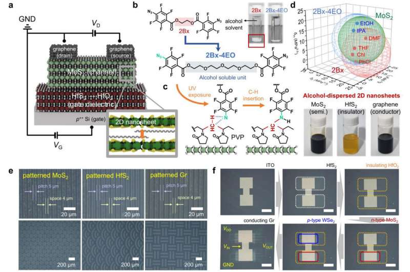
The innovation lies in combining 2D nanomaterials such as molybdenum disulfide (MoS₂) with a UV-curable cross-linker dispersed in an alcohol-based solvent. Unlike traditional fabrication techniques that rely on toxic organic solvents, this approach uses isopropanol—an environmentally safer alternative—to precisely define and solidify circuit patterns using ultraviolet light. The unreacted material is simply rinsed away with water, leaving behind clean, sharply defined 2D semiconductor structures.
2D materials like MoS₂ are prized for their atomically thin, layered structure, which offers superior electronic performance and energy efficiency. However, their fragile nature makes them difficult to process using conventional deposition or etching methods. The new method resolves this challenge by introducing a room-temperature, solvent-based photopatterning process that avoids structural damage.
The team, led by Professor BongSoo Kim of UNIST along with Professors Joohoon Kang and Jeong Ho Cho of Yonsei University, fine-tuned the chemistry of azide-based cross-linkers to make them soluble in isopropanol—something previously thought impossible. This adjustment allowed stable dispersion of 2D materials and efficient UV-induced cross-linking, ensuring uniform and reproducible circuit formation.
Performance tests demonstrated the method’s technical viability. Fabricated MoS₂ transistors showed a charge carrier mobility of 20.2 cm²/V·s, a threshold voltage of 2.0 V, and an on/off ratio of 2.7 million. Arrays of 49 transistors maintained stable operation for over 60 days, and the process enabled the creation of both p-type and n-type semiconductor circuits, including NOT, NAND, NOR gates, and SRAM cells. By extending UV cross-linking technology—previously used in quantum dot displays—to 2D materials, this technique marks a critical step toward greener, scalable, and high-precision semiconductor manufacturing.