Paving the way for students, researchers, and startups alike, India’s chip designers can now turn ideas into real silicon using open source tools on an Indian process node.
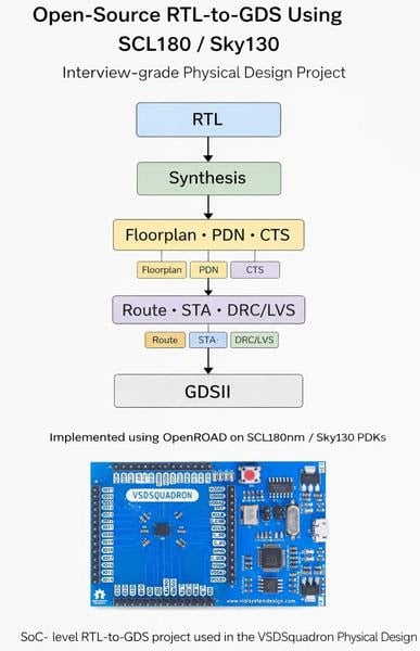
A milestone for India’s semiconductor ecosystem, VSD (VLSI System Design) has successfully demonstrated a working open source RTL-to-GDS flow on the Indian SCL 180 nm process node. For a long time, access to advanced chip design tools has been a barrier for many students and researchers in India, particularly those at tier II, III, and IV colleges, who have access to Indian process design kits (PDKs) but lack high-end proprietary electronic design automation (EDA) tools. This achievement enables designers to take a digital design from RTL (register transfer level) to GDSII (graphic data system ii), the final layout file required for chip fabrication, using open source EDA tools mapped to an Indian PDK.

By mapping the SCL 180 nm PDK into an open RTL-to-GDS flow, VSD has shown that Indian process technologies can be fully integrated into modern open source design ecosystems. This involved extensive customisation of track definitions, power delivery network (PDN) strategies, tap and filler cells, and design rule check/extraction (DRC/RCX) configurations. It is like proof that Indian PDKs are not merely academic resources but silicon-ready platforms compatible with real-world design flows.
“This opens up an entire learning path for students aspiring to design and tape out chips within India,” said Kunal Ghosh, founder of VSD. Traditionally, full-chip implementation flows require expensive commercial toolchains, limiting hands-on silicon experience to select institutions and large companies. With this development, students, researchers, startups, and engineering teams can now experience an end-to-end silicon-oriented workflow, from RTL coding to physical implementation, within India’s own semiconductor framework.

This initiative strongly supports the broader goal of strengthening India’s semiconductor design ecosystem and building sovereign capability. It reduces dependence on proprietary tool stacks, democratises access to chip design infrastructure, and enables deeper engagement with Indian foundry technologies.
Beyond providing tools and scripts, the true impact is in transforming talent. For students, it bridges the gap between theory and fabrication. For researchers, it enables rapid prototyping and silicon validation. For startups, it lowers the barriers to entering ASIC development. At a national level, it reflects growing maturity in the design infrastructure.
India has always had the talent. What was needed was accessible infrastructure. With a working open RTL-to-GDS flow on an Indian process node, the journey from idea to silicon is no longer distant; it is achievable. For every Indian engineer who dreams of building chips that carry the mark “Designed in India,” this milestone is more than technical progress; it is a testimony that the foundation is being laid at home.