Achieve the perfect balance between efficiency, noise performance, and miniaturisation—enabling reliable power solutions for next-generation portable and battery-powered devices.
It serves as an important benchmark for design engineers working on compact, battery-powered electronics, especially in wearable and IoT systems. Its significance lies in demonstrating how to achieve an optimal balance between efficiency, noise performance, and miniaturisation—three critical parameters in modern embedded design. This reference design is widely applicable in devices such as smartwatches, earbuds, smartphones, AR/VR systems, GPS modules, and portable medical electronics, where clean power delivery directly affects signal integrity and system reliability. For a design engineer, it provides a practical blueprint for designing ultra-low-noise power rails capable of supporting sensitive analog and RF loads while maintaining long battery life. The architecture is especially valuable in applications involving sensors, wireless communication modules (Bluetooth, NB-IoT), and data converters, where power supply noise can significantly degrade performance.

The TIDA-01566 reference design is centred around a hybrid power architecture that combines a DC/DC buck converter with a low-dropout (LDO) regulator to leverage the strengths of both technologies. The DC/DC converter provides high efficiency, particularly at moderate to high loads, while the LDO ensures ultra-low output noise by filtering switching ripple from the converter. This combination enables the design to achieve near-LDO-level noise performance (~100 µV) while maintaining significantly higher efficiency than an LDO-only solution. The system operates within an input voltage range of approximately 2.6 V to 5.5 V and delivers a stable 1.2 V output, making it suitable for single-cell lithium battery-powered devices.
A key engineering insight from this design is its ability to maintain ultra-low quiescent current (around 8 µA), which is critical for extending battery life in standby or light-load conditions.
The DC/DC converter operates in power-save mode to reduce switching losses, but this introduces ripple at lower frequencies. The subsequent LDO stage effectively attenuates this ripple due to its high power supply rejection ratio (PSRR), ensuring clean power for sensitive components. This layered approach demonstrates an important design trade-off—using multiple stages to optimise both efficiency and noise, rather than relying on a single regulator type.
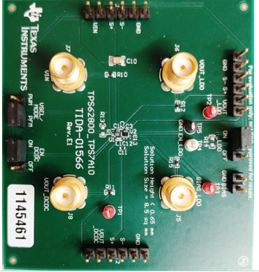
Another notable feature is the extremely compact implementation, with a total solution size of about 8.5 mm² and very small passive components. This highlights the importance of PCB layout optimisation and component selection in high-density designs. Engineers can learn how package selection (such as wafer-scale chip packages) and high-frequency switching enable smaller filters, contributing to overall miniaturisation without compromising performance.
From a system design perspective, TIDA-01566 also provides comparative insights between three architectures: DC/DC-only, LDO-only, and hybrid DC/DC + LDO. It shows that while DC/DC converters offer higher efficiency, they introduce more noise; conversely, LDOs provide cleaner output but are less efficient. The hybrid approach emerges as the best compromise for many modern applications.
It serves as a valuable learning model for design engineers by illustrating how to systematically address real-world constraints such as power efficiency, noise sensitivity, thermal performance, and space limitations. It not only provides ready-to-use design files and schematics but also offers deep insights into architectural trade-offs, making it an essential reference for developing next-generation portable electronic systems. For more information, click here.