

With 97.6% device yield and ultra-low variation, this advancement could finally unlock mass manufacturing for next-gen atom-thin electronics.
Two-dimensional (2D) semiconductors—atom-thin materials like molybdenum disulfide (MoS₂)—are widely hailed as the next silicon. But turning their lab-scale promise into mass-produced electronics has hit a persistent snag: scalable, clean, and damage-free patterning. Conventional methods often involve harsh chemicals or polymer masks that can leave behind residue or degrade the fragile films.
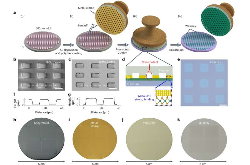
Now, researchers at Nanyang Technological University (NTU), Singapore, have delivered a potential game-changer: a novel imprinting technique that uses a metal stamp with a 3D microstructure to pattern 2D materials directly onto wafers—without chemical processing or mechanical damage.Here’s how it works: a precisely engineered stamp is pressed onto a 2D semiconductor film grown on a substrate. Upon removal, the stamp lifts only the areas it contacts, cleanly peeling off selective regions and leaving behind pristine, patterned arrays. The key? Localized contact and exfoliation at the nanoscale—no etching, no polymers, no contamination.

Characterization of the patterned films revealed intact crystal structures and clean surfaces. But NTU didn’t stop at lab validation—they fabricated hundreds of MoS₂-based transistors using this method and ran the numbers.The result: 20× less variation in threshold voltage compared to traditional reactive-ion etching, and a 97.6% device yield across a 2-inch wafer. That’s serious industrial potential.
If further scaled and adopted, this residue-free stamping approach could help 2D semiconductors finally leap from experimental setups into next-gen chips powering everything from ultra-efficient smartphones to edge AI devices. Better still, it’s fully compatible with today’s semiconductor fab workflows. As the industry inches closer to the post-silicon era, this clean, scalable patterning technique could prove to be the missing puzzle piece. “Despite progress in 2D material synthesis, residue-free patterning has held us back,” the team writes in Nature Electronics. “Our method removes this bottleneck.”