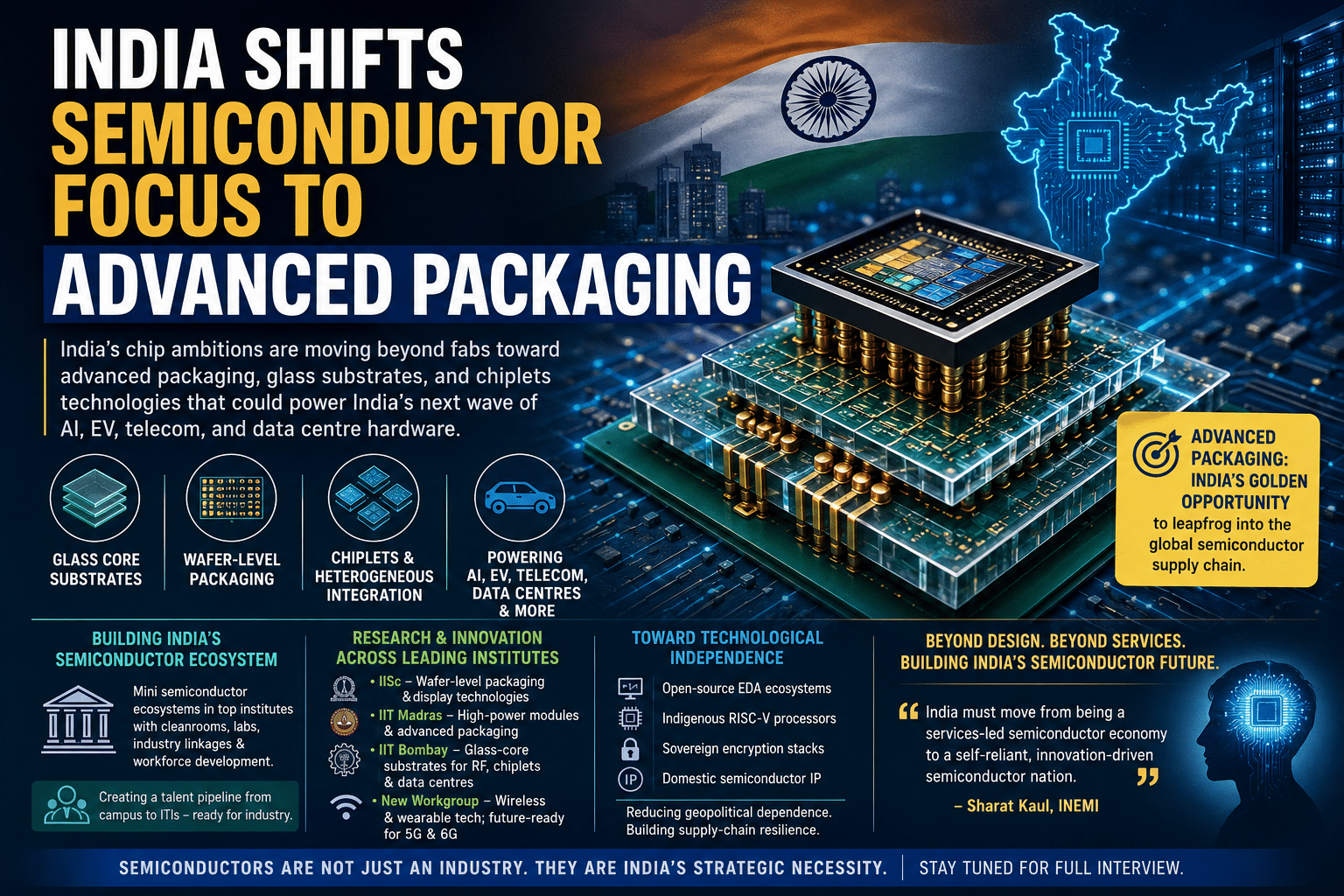
India’s chip ambitions are moving beyond fabs toward advanced packaging, glass substrates, and chiplets technologies that could power India’s next wave of AI, EV, telecom, and data centre hardware.
India’s semiconductor ambitions are increasingly shifting beyond fabs toward advanced packaging, glass substrates, wafer-level packaging, and indigenous chip ecosystems. In an exclusive conversation, Sharat Kaul of INEMI shared with EFY’s Akanksha Sondhi Gaur that he believes the country’s biggest weakness is not engineering capability, but the missing link between semiconductor design and manufacturing. While India has become a global hub for semiconductor design services, much of the high-value manufacturing, packaging, materials, and process ownership still remains outside the country.

India exports semiconductor talent but imports the actual semiconductor products, manufacturing technologies, and supply chain control. This has created what Kaul describes as a “services-led semiconductor economy,” in which Indian engineers design chips for multinational companies, while the intellectual property, packaging infrastructure, and production ecosystems remain concentrated overseas. To address this, INEMI India is now pushing an “advanced packaging-first” approach to help India become relevant in the next phase of semiconductor manufacturing without waiting decades to compete at bleeding-edge fabrication nodes.
The strategy focuses on areas such as glass-core substrates, wafer-level packaging, integrated power modules, heterogeneous integration, chiplet-ready architectures, RF packaging, and next-generation semiconductor materials. Kaul described advanced packaging as India’s “golden opportunity” to leapfrog into the global semiconductor supply chain. Instead of directly competing with global leaders in sub-5nm fabrication, India is attempting to build expertise in the backend technologies that will define future electronics, AI hardware, electric vehicles, data centres, telecom systems, and wearable devices.
To accelerate this effort, INEMI India has already established multiple semiconductor working groups across leading institutes. Indian Institute of Science is working on wafer-level packaging and display technologies, while IIT Madras is focused on high-power semiconductor modules and advanced packaging lines. IIT Bombay is developing glass-core substrate technologies, which are expected to become increasingly important for RF systems, data centres, and chiplet-based architectures. A fourth workgroup focused on wireless technologies and wearable electronics is also being planned, with future expansion toward 5G and 6G ecosystems.
One of the most significant developments emerging from these initiatives is the creation of localised “mini semiconductor ecosystems” inside universities and technical institutions. These ecosystems combine cleanrooms, reliability labs, packaging experimentation facilities, industry-linked training, and workforce development programs. Kaul revealed that some of these pilot initiatives have already achieved full placement of trained students into electronics manufacturing companies. The larger objective is to create a nationwide semiconductor talent pipeline that extends beyond elite engineering institutions to technician-level infrastructure, such as ITIs.
He also highlighted a broader strategic concern driving these efforts: geopolitical dependence. India currently imports most of its advanced processors, semiconductor-grade materials, EDA software, packaging equipment, and microcontrollers. To reduce that dependence, India is simultaneously exploring open-source EDA ecosystems, indigenous RISC-V processors, sovereign encryption stacks, and domestic semiconductor IP development. Semiconductors are no longer simply an industrial opportunity, but a strategic necessity tied directly to national security, supply-chain resilience, and long-term technological independence.
Stay tuned for the full interview.