
A new technique from the University of Strathclyde allows ultra-small photonic devices to be measured, sorted, and assembled with unprecedented accuracy—unlocking scalable manufacturing for advanced optical systems in quantum tech, AI, and next-gen telecom.

Researchers at the University of Strathclyde have pioneered a method for assembling ultra-small, light-manipulating devices—photonic crystal cavities (PhCCs)—with unmatched precision. These microscopic structures trap and guide light and are foundational for cutting-edge technologies like quantum computing, AI-driven photonics, high-speed telecoms, and next-gen sensing platforms.
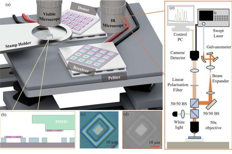
Traditionally, building arrays of PhCCs on a single chip faced a major barrier: even nanometer-scale imperfections during fabrication altered each unit’s optical behavior, rendering large-scale integration nearly impossible. Strathclyde’s new approach overcomes this limitation by physically removing individual PhCCs from their original silicon wafer and transferring them to a target chip—while simultaneously measuring and sorting them in real time by their resonant wavelength.

At the heart of this innovation is a custom-built semiconductor integration platform that can identify, handle, and place PhCCs with sub-micron accuracy. This allows researchers to “see” and select each device’s performance before final placement—much like choosing the exact color of Lego bricks before building a model, instead of guessing mid-assembly.
In a single session, the team successfully assembled 119 PhCCs into a perfectly tuned array—something previously deemed impossible due to fabrication-induced variances. The process not only ensures consistency but also reveals, for the first time, how these delicate devices physically react during integration, uncovering mechanical effects like stress and deformation that play out over seconds to hours.
Dr. Sean Bommer, lead author, highlights the leap: “For the first time, we can characterize photonic performance during integration. It’s a game-changer for photonic design.”
Professor Michael Strain, Fraunhofer and RAEng Chair in Chipscale Photonics, adds: “This gives us the power to rearrange microscopic photonic elements after fabrication, unlocking scalable, hybrid chip architectures. Our next step is integrating a variety of semiconductor devices on a single chip—bringing quantum, telecom, and sensor technologies into a new era of complexity and performance.”